工程师接受在线咨询

|
|
Wafer Alignment, Dicing, and Assembly |
|
|
Pick-and-Place (P&P) and Chip Shooting |
|
|
Automated Optical Inspection (AOI) |
|
|
Flat Panel Inspection |
Accurate and reliable machine vision components are an absolute requirement for all steps in the inspection and assembly of electronics and semiconductors, including wafer probing and dicing, wire bonding and chip flipping, and device assembly.
Microlithography is used to manufacture semiconductor wafers. Once aligned, the wafers are diced into chips and assembled, along with additional components, into electronics devices like integrated circuits. Chips are deposited onto circuit boards using pick-and-place (P&P) robots or chip shooters. Chip placement on the board is monitored by automated optical inspection (AOI) systems. Individual chips and components are then soldered together with a ball grid array or other advanced techniques in a factory automation environment.
As Moore’s Law has shown over the last few decades, the number of transistors on integrated circuits has been doubling every two years. Additional transistors require additional computing and processing power. Computer, smartphone, and other electronics manufacturers then make use of this additional processing power by offering faster speeds, better graphics, and overall improvements in the next generations of products. While it is assumed that some electronics markets will eventually reach saturation, thousands of millions of electronic consumer goods like smartphones are sold each year and will likely continue to sell for the foreseeable future.

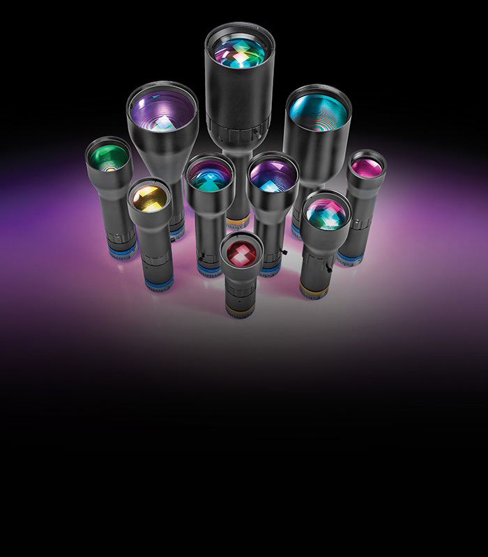
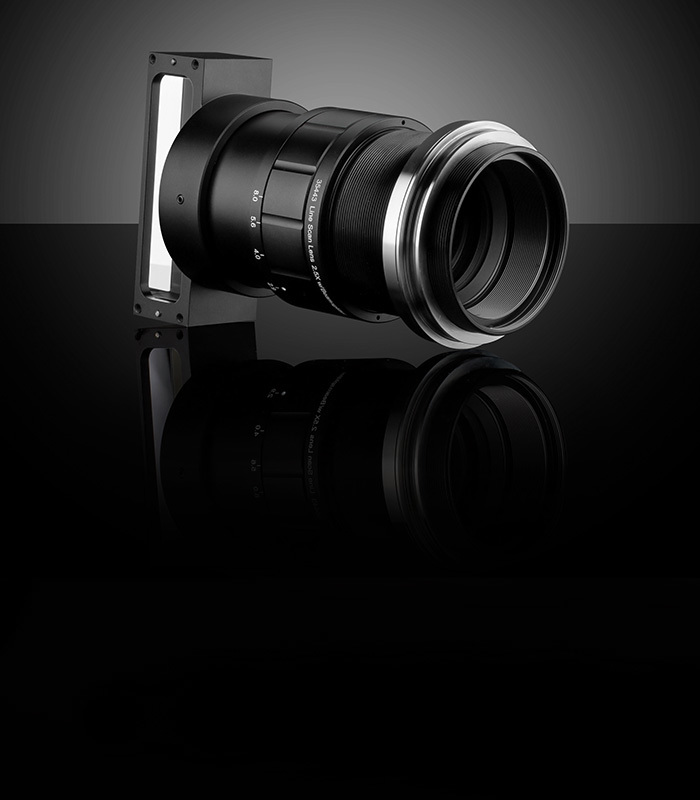
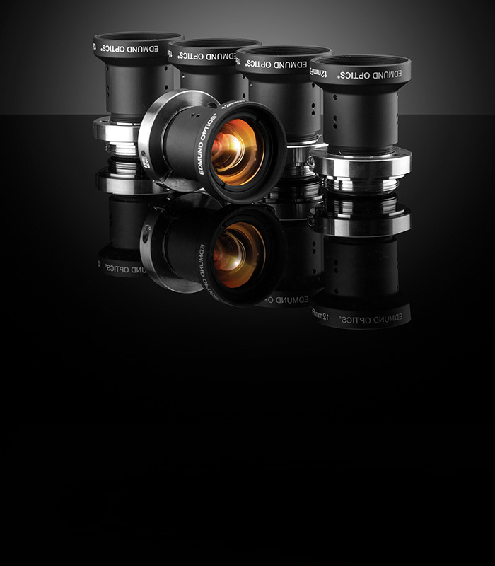
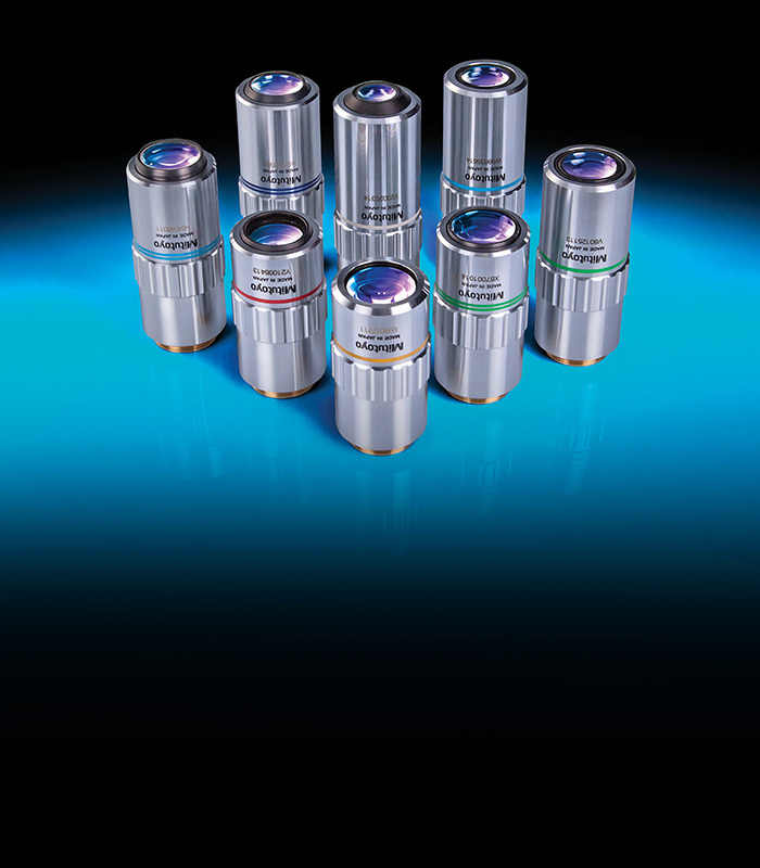
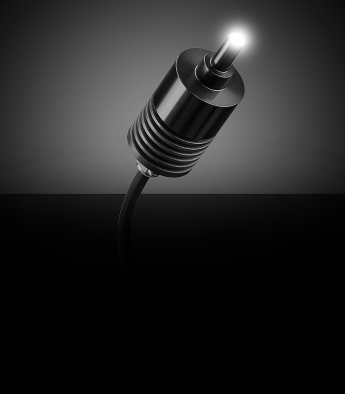
Machine vision lenses, including telecentric lenses, low distortion fixed focal length lenses, line scan lenses, and microscope objectives, are often used in semiconductor production with inline illumination to observe and align semiconductor wafers during microlithography.
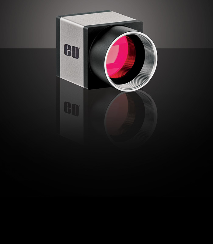
These machine vision lenses, along with illumination sources like ring or spot lights, are used in automated optical inspection (AOI) systems that perform visual inspection of electronic chips, flat panel displays, and many more electronic components. AOI systems monitor attributes like chip placement and orientation with respect to the entire board and the depth or height of layered devices, such as CMOS sensors. AOI systems also ensure that connecting leads are slotted into the correct ports.
Edmund Optics (EO) is a world class optics and photonics manufacturer with over 78 years of experience in optics, design, testing, and manufacturing. Additionally, EO offers a broad selection of versatile and off-the-shelf products, which are continuously updated to support current, relevant challenges for electronics & semiconductors inspection. Learn more about Edmund Optics and our World-Class Imaging Optics and Manufacturing Capabilities.
1 O'Dea, S. “Cell Phone Sales Worldwide 2007-2020.” Statista, 28 Feb. 2020, www.statista.com/statistics/263437/global-smartphone-sales-to-end-users-since-2007/.


或查看各区域电话
报价工具
只需输入商品编号
Copyright 2023, 爱特蒙特光学(深圳)有限公司。— 广东省深圳市龙华工业东路利金城科技工业园3栋5楼 518109 - 粤ICP备2021068591号